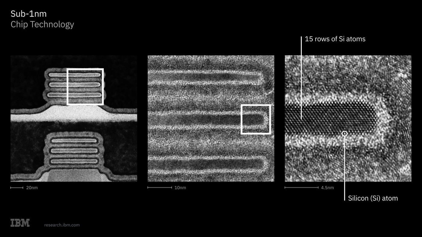
IBM Unveils World's First 0.7nm Chip, Packing Nearly 100 Billion Transistors Onto a Fingernail-Sized Die
The world's first sub-1 nanometer logic chip
For over 40 years, chips have advanced by shrinking transistors smaller and smaller — now the size is closing in on a single atom. This is the first time the industry has crossed below 1 nanometer, and IBM's method isn't more shrinking — it's stacking transistors vertically instead.
To understand this breakthrough, first see how hard the wall really is
Crossing below 1 nanometer is a milestone because the old path was genuinely running out of road. For decades, chips got better through one straightforward move: make transistors smaller so more fit on the same chip, pushing compute and efficiency up together. The problem is transistor sizes are now approaching the scale of a single atom — there's barely any room left to keep shrinking on a flat plane. The "just make it smaller" path is nearly played out.
Primary source and reference
- IBM Newsroom Original publisher